MEMS PCB
Chip Device
Chip LED PCB (prototype to mass production)
Thin PCB
Thickness of 0.06 – 0.6mm.
Using BT resin material to realize stable mechanical properties and reliable insulation.
Edge Circuit PCB
Form circuit pattern on the edge of the PCB.
Less crack or burr from traditional edge through hole PCB to realize smaller size.
Cavity Structure PCB
Bond edge circuit PCBs stick together and mount a device into the cavity area to realize a flat PCB after mounting.
Device PCB
Package PCB with molding a device by resin onto the PCB and connect with wire bonding for electrical connection. Lighting is the main application.
Other PCBs
Other than above, we come up with various solutions.
Feel free to contact us anytime.
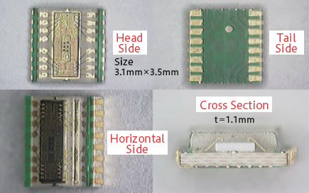
Sensor PCB Chip installed picture (actual size)
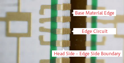
Photo detectors PCB edge circuit picture