Flat Plug PCB (Permanent Hole-filling PCB)
Features
- With screen printing method, selected through holes are filled with resin and protect the through holes.
- With special polishing, it does not affect surface mounting.
- UL acquired : Only for multi-layer PWB (4 or 6 layers) (Contact us for further inquiry)
Product Pictures
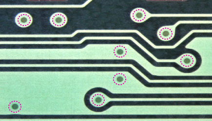
Picture after solder resist painted
Product Specifications
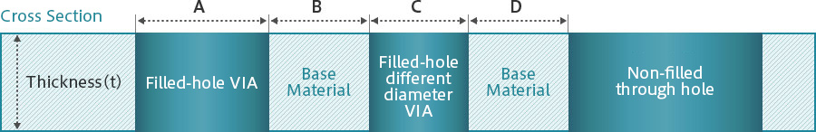
| Item | Symbol | Standard Spec | Note |
|---|---|---|---|
| Base Material | - | FR-4( R-1766 ) | UL compatible: 4 or 6 layers and CEM-3 |
| Thickness | t | 0.80 – 1.60 [mm] | |
| Resin Filled Diameter (Final Diameter) |
A | φ0.20 – 0.50 [mm] | |
| Resin Filled VIA min. distance | B | More than 0.55 [mm] | |
| Resin Filled VIA diameter difference | A-C | Less than 0.20 [mm] | When there are more than two different diameters for resin fill |
| Aspect Ratio | - | Less than 8.0 | t/A |
| Distance between filled VIA and through hole | D | More than 0.425 [mm] | |
| Surface treatment | - | OSP | Sn, Pb or Pb-free solder level, gold plating compatible |
Product Properties
| Item | Test Condition / Judge Standard | Results |
|---|---|---|
| Cooling/heating cycle test result | -65 °C / 30 min : 125 °C / 30 min : 100 After 100 cycles | 1. Change rate of conductor resistivity: Ave. 1.18% 2. No problem |
| 1. Change rate of conductor resistivity less than 10% 2. No change on appearance, no crack, no problem with adhesion |
||
| Solder heat resistance test result | 40 °C / 90 %Rh / 96 Hr : After 2 cycles of dipping into Pb-free solder 260°C / 20sec |
1. Change rate of conductor resistivity: Ave. 1.23% 2. No problem |
| 1. Change rate of conductor resistivity less than 10% 2. No change on appearance, no crack, no problem with adhesion |
||
| Chemical resistance test result | Soak into soft etching solution (sulfuric acid - hydrogen peroxide) for 180 seconds : 40 °C / 93 %Rh / 240 Hr |
1. Change rate of conductor resistivity: Ave. 0.09% 2. No problem |
| 1. Change rate of conductor resistivity less than 10% 2. No change on appearance, no crack, no problem with adhesion |
Above numbers are actual measurements as a reference, not assurance of quality.