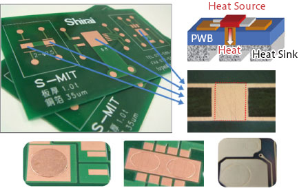
Cu-Inlay PCB "S-MIT®"
Features
- Taking advantage of copper's high thermal conductivity,
- Transform the heat from the heated device onto the backside.
- Light-weight design as the copper is only inserted where heat management is needed.
On-spot heat dissipation
| Item | Standard Specification | Note |
|---|---|---|
| Base | FR-4 35 [μm] | Compatible with CEM-3, halogen-free, high Tg material |
| Thickness | 1.0, 1.6[mm] | Compatible with 0.6 – 1.6mm |
| Cu-Inlay Diameter | φ2.5, 5.0, 8.0[mm] | Please contact us for other diameters. |
| Cu-Inlay Distance | More than board's thickness | Please indicate where to insert the copper in the drawings. |
| Cu-Inlay Shape | Round Circle | Please contact us for other special shapes such as square, etc. |
| Cu-Inlay Insert Process | Post NC drill or post Cu plating | Standard: Cu plating : Cu-Inlay insertion : pattern form |
| Surface Treatment Specification | OSP | Also compatible with Pb-free solder level, Ni-Au plating. |
Features
| Item | Test Condition | Results |
|---|---|---|
| Pin Unevenness | Temperature cycle(-65±3[°C] 30[min] 125±3[°C] 30[min]) : Post 500 cycle |
A-side: Within +0.03 – 0.05 B-side: Within +0.10 – -0.05 |
| Pin Retention | Retention temperature cycle(-65±3[°C] 30[min] 125±3[°C] 30[min]) : Post 500 cycle |
Pin condition: Not fallen off |
| SMT Endurance | Preprocess(40[°C]/90[%]/96[Hr]) : Post twice SMT mounting |
No floating of pattern, delamination or inflation |
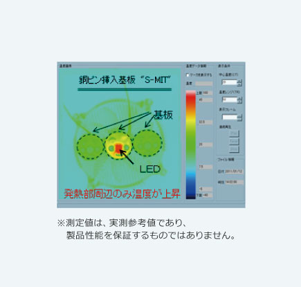
Above numbers are actual measurement, not assure the specification.
Structure
"S-MIT®" (Shirai Metal Insertion Technology PWB) is a registered trademark of Shirai Electronic Industrial, Co., Ltd.
Patented (No. 5788854)